
Download Gowin EDA (FPGA Designer) 1.9.12 – Comprehensive FPGA Development Environment
Gowin EDA (FPGA Designer) 1.9.12 is an integrated development environment developed by Gowin Semiconductor, specifically designed for their range of FPGA and SoC products. This comprehensive suite supports the entire FPGA design flow, from initial concept through to final bitstream generation for programming. It is an essential tool for electronics engineers, embedded systems developers, and professionals involved in hardware prototyping and digital logic design, offering a cost-effective solution for designing with Gowin’s efficient FPGA architectures.
An Overview of Gowin EDA and Its Role in FPGA Design
Gowin EDA serves as Gowin Semiconductor’s proprietary Electronic Design Automation (EDA) solution, offering a unified platform for developing sophisticated digital logic circuits on FPGAs. Unlike general-purpose EDA tools, Gowin EDA is deeply optimized for Gowin’s specific FPGA architectures, ensuring efficient synthesis, place-and-route, and timing closure. This specialization is crucial for maximizing the performance and minimizing the power consumption of devices, making it a valuable asset in fields like embedded systems development, where performance and efficiency are paramount. The software provides a complete workflow, empowering users to take a design from an idea to a physical implementation on an FPGA.
Design Workflow and Tools Provided by Gowin EDA
Gowin EDA facilitates a structured design process by offering a suite of integrated tools that cover all essential stages of FPGA development. From initial logic definition to final verification, the environment is built to support complex project requirements efficiently.
Design Entry: HDL and Schematic Capture
The Gowin EDA environment includes a robust text editor with advanced features tailored for hardware description languages (HDLs). It provides comprehensive support for Verilog, VHDL, and SystemVerilog, enabling designers to express complex digital logic using their preferred HDL. Additionally, for users who prefer a graphical approach, Gowin EDA offers a block schematic capture utility. This allows for the visual creation and interconnection of logic blocks, which can be particularly useful for simpler designs or for hierarchical design methodologies.
IP Core Generation for Efficient Designs
To accelerate the design process and promote the reuse of complex functionalities, Gowin EDA incorporates an IP Core Generator. This feature provides ready-to-use, pre-verified intellectual property blocks that are essential for many modern FPGA applications. Common IP cores available through this generator include Phase-Locked Loops (PLLs) for clock management, memory controllers for interfacing with external memory devices, and standard processor cores for System-on-Chip (SoC) implementations. Utilizing these pre-built IP blocks significantly reduces design time and the risk of introducing errors.
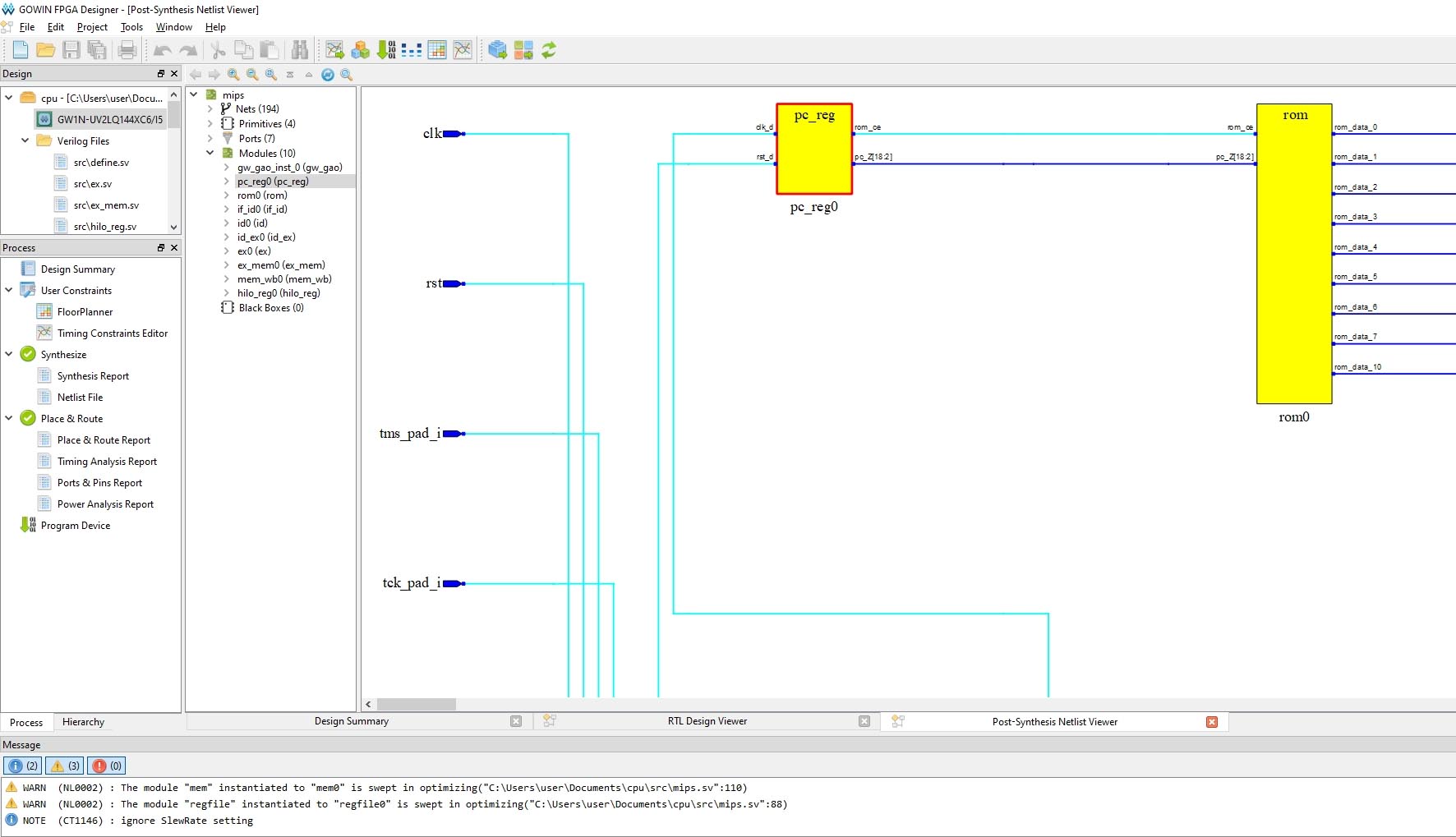
Synthesis, Implementation, and Timing Analysis Optimized for Gowin FPGAs
The critical stages of translating high-level HDL code into a hardware implementation are handled by Gowin EDA’s specialized internal tools, which are fine-tuned for Gowin’s proprietary FPGA architectures. This optimization is key to achieving performance targets and managing resource utilization effectively.
The heart of the implementation flow is GWINSYN, Gowin’s proprietary synthesis engine. It parses the HDL code and logic designs to create an optimized netlist, mapped to the specific primitives available on Gowin FPGAs. Following synthesis, the place-and-route tools determine the optimal physical location for each logic element and the routing paths between them on the FPGA fabric. This process is guided by the design’s constraints and aims to minimize critical path delays. To ensure the design meets its performance requirements, Gowin EDA includes a Static Timing Analysis (STA) tool. STA analyzes all possible signal paths within the design against user-defined timing constraints, reporting any violations, such as setup or hold time issues, that could prevent the design from operating correctly at the target clock frequency.
Simulation and Verification Capabilities
Accurate simulation and verification are indispensable for confirming the functional correctness of an FPGA design before it is programmed onto hardware. Gowin EDA provides integrated tools to support this crucial phase, allowing designers to build confidence in their logic.
The environment includes an integrated waveform viewer, which is used to display and analyze the simulation results. This tool allows designers to observe the behavior of signals over time, compare them against expected outcomes, and identify any functional bugs. While Gowin EDA offers robust internal simulation capabilities, it also maintains compatibility with industry-standard third-party simulators, such as Mentor Graphics’ ModelSim. This compatibility ensures that users can leverage familiar simulation tools or more advanced verification methodologies if their project demands it.
Programming and In-System Debugging Tools
Once a design has been synthesized, placed, routed, and verified through simulation, Gowin EDA provides the necessary tools to program the target FPGA and debug it in real-world operation. This enables a seamless transition from the design environment to physical hardware testing.
The Gowin Programmer is an integral part of the suite, responsible for generating the final bitstream file required to configure the FPGA. This tool interfaces with Gowin’s programming hardware to load the design onto the FPGA device. For hardware debugging, Gowin EDA features a powerful in-system logic analyzer. This tool is invaluable for understanding the actual behavior of the design running on the FPGA. It allows designers to select and probe internal signals within the FPGA in real-time, observe their values as the circuit operates, and correlate this behavior with external stimuli or outputs, greatly simplifying the process of identifying and resolving hardware-level issues.
Advantages and Use Cases of Gowin EDA in Industry and Education
Gowin EDA offers significant advantages, particularly regarding cost-effectiveness and specialized optimization, making it an attractive choice for a wide range of users.
A major benefit is that Gowin EDA is provided completely free of charge, with full features and no artificial restrictions on design complexity or usage. This makes it an exceptionally cost-effective solution for startups, small to medium-sized businesses, individual hobbyists, and educational institutions that might otherwise face significant licensing costs for comparable professional EDA tools. The deep optimization for Gowin’s FPGA architectures ensures that users can achieve high performance and power efficiency tailored to their devices. With support for multiple interface languages, including English and Chinese, the tool is accessible to a global user base. These factors combine to make Gowin EDA an ideal platform for embedded system prototyping, rapid hardware development, and comprehensive digital logic design education.
Frequently Asked Questions
What FPGA programming languages does Gowin EDA support?
Gowin EDA supports major hardware description languages including Verilog, VHDL, and SystemVerilog, enabling flexible design entry for a variety of FPGA projects. This broad language support allows engineers to utilize their existing expertise and choose the most appropriate language for their specific design needs.
Is Gowin EDA free to use for commercial projects?
Yes, Gowin EDA is provided free of charge with registration and includes full features without restrictions, making it suitable for both commercial and educational use. This cost-free model democratizes access to advanced FPGA design tools, benefiting startups and commercial ventures.
Can Gowin EDA be used for debugging running FPGA designs?
Yes, it includes an in-system logic analyzer that allows real-time probing of internal FPGA signals during operation, which is essential for verification and debugging of complex designs. This capability significantly aids in troubleshooting and optimizing the behavior of hardware implementations.


Reviews
There are no reviews yet.