
Download Xilinx Vivado Design Suite 2024.2.1 – Advanced FPGA and SoC Design Environment
The Xilinx Vivado Design Suite 2024.2.1 is an advanced, integrated electronic design automation (EDA) environment developed by Xilinx, a subsidiary of AMD, for designing and implementing hardware on Xilinx Field-Programmable Gate Arrays (FPGAs) and System-on-Chips (SoCs). It provides a comprehensive platform for engineers in sectors such as embedded systems, aerospace, automotive, defense, and signal processing who require robust tools for modern hardware development. This suite is engineered to accelerate time-to-market for complex digital designs through its scalable, modular approach.
Overview of Vivado Design Suite for FPGA and SoC Development
Xilinx Vivado Design Suite represents a significant evolution in FPGA and SoC design environments, succeeding previous Xilinx tools by offering a unified platform for the entire design flow. This integrated suite supports the latest Xilinx FPGA device families, including UltraScale, Versal, and Zynq, enabling the development of sophisticated hardware solutions. Vivado is tailored for professional engineers working on complex projects, facilitating advanced hardware logic implementation and system-on-chip integration.
Design and Synthesis Capabilities in Vivado
Integrated RTL and High-Level Synthesis
Vivado Design Suite supports multiple design entry methods, allowing engineers to work with Register Transfer Level (RTL) code or leverage High-Level Synthesis (HLS) to create designs from C, C++, or SystemC. The HLS capability converts these high-level descriptions into optimized RTL, significantly accelerating the design cycle for complex algorithms and reducing the manual effort traditionally associated with hardware design.
IP Integration and System-Level Design
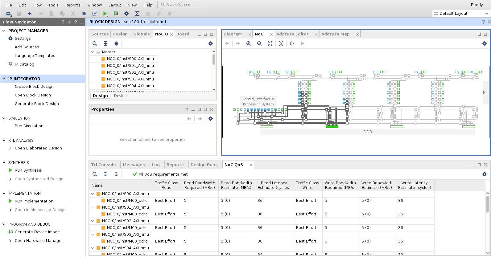
The suite features the IP Integrator, a graphical environment that simplifies system-level design by allowing the integration of pre-designed, reusable Intellectual Property (IP) cores. It supports industry-standard interfaces, including the Advanced eXtensible Interface (AXI) protocol, facilitating easy connection of various components and enabling complex hierarchical design flows for scalable FPGA and SoC projects.
Advanced Analysis, Debugging, and Simulation Features
Timing and Power Analysis
Vivado provides in-depth timing analysis tools to help ensure that designs meet performance requirements, offering insights into propagation delays and critical paths. Complementing this, advanced power analysis features provide estimations and insights into static and dynamic power consumption, enabling designers to optimize energy efficiency. Constraint management is also integral, allowing precise control over design parameters.
Real-Time Hardware Debugging Tools
For effective hardware validation, Vivado includes powerful debugging capabilities. The Vivado Logic Analyzer allows engineers to observe and analyze internal signals within the FPGA in real-time, directly from the hardware. Additionally, the Serial I/O Analyzer provides dedicated tools for debugging high-speed serial communication interfaces, crucial for complex system integration.
Simulation Environment Support
The design process in Vivado is supported by a robust simulation environment. It offers the integrated Vivado Simulator for fast and accurate simulation of designs, as well as compatibility with industry-standard simulators like Mentor Graphics ModelSim. This ensures thorough verification of design functionality before and after hardware implementation.
Device and Platform Compatibility
The Xilinx Vivado Design Suite is optimized to work with a broad range of Xilinx FPGA and Adaptive Compute Acceleration Platform (ACAP) devices. This includes popular families such as Artix, Kintex, Virtex, diverse Zynq SoC devices (including Zynq-7000 and Zynq UltraScale+ MPSoC), and the advanced Versal ACAPs. The software also supports multi-platform operating systems, including Windows and Linux, and integrates with cloud-based workflows for enhanced accessibility and scalability, accommodating modern development practices.
Practical Applications and Industry Use Cases
Vivado Design Suite is instrumental in a variety of demanding applications across multiple industries. It is heavily utilized in the design of embedded systems, offering solutions for real-time processing and control. In the aerospace and defense sectors, it facilitates the development of mission-critical systems requiring high reliability and performance. The automotive industry benefits from its capabilities in designing advanced driver-assistance systems (ADAS) and infotainment platforms. Furthermore, Vivado is increasingly vital for AI hardware acceleration, enabling the creation of specialized processors for machine learning tasks, and is extensively used in high-speed signal processing for telecommunications.
Customization, Automation, and Extensibility
To enhance design efficiency and manage complex workflows, Xilinx Vivado Design Suite offers extensive customization and automation capabilities. Engineers can utilize Tcl scripting to automate repetitive tasks, customize build processes, and integrate Vivado into broader design automation flows. The platform’s modular architecture and support for user-defined constraints further allow for fine-grained control, enabling tailored optimization for specific design requirements and performance targets.
Frequently Asked Questions
What FPGA devices are supported by Xilinx Vivado Design Suite 2024.2.1?
The Vivado Design Suite supports a wide range of Xilinx FPGA families including Artix, Kintex, Virtex, the Zynq-7000 and Zynq UltraScale+ MPSoC, as well as the latest Versal Adaptive Computing Acceleration Platform (ACAP). This broad compatibility ensures that engineers can utilize Vivado with their chosen Xilinx hardware for diverse project needs.
How does Vivado’s High-Level Synthesis (HLS) improve FPGA development?
Vivado’s HLS allows developers to write designs in high-level languages such as C, C++, and SystemC, which it then converts into optimized RTL code. This accelerates development cycles by enabling faster iteration and reduces the complexity of hardware design, making it more accessible and efficient for a wider range of engineers.
Can Vivado Design Suite be used for real-time hardware debugging?
Yes, Vivado includes built-in debugging tools such as the Vivado Logic Analyzer and Serial I/O Analyzer, which enable real-time observation and analysis of FPGA signals, helping engineers troubleshoot and validate hardware behavior effectively. These tools are essential for ensuring the correct functionality of complex FPGA designs in a live environment.


Reviews
There are no reviews yet.