
Download Z-planner Enterprise 2025.1 – Advanced PCB Stackup Design and Signal Integrity Software
Z-planner Enterprise 2025.1 is a specialized PCB stackup planning software designed for engineers working with high-speed digital and RF board designs. It leverages advanced field-solver technology to provide precise modeling of electromagnetic behavior within multilayer Printed Circuit Boards (PCBs). This tool is essential for signal integrity engineers, PCB design leads, RF engineers, and fabrication engineers who require accurate simulation and manufacturability data for complex electronic products.
Precision Stackup Planning for High-Speed PCB Designs
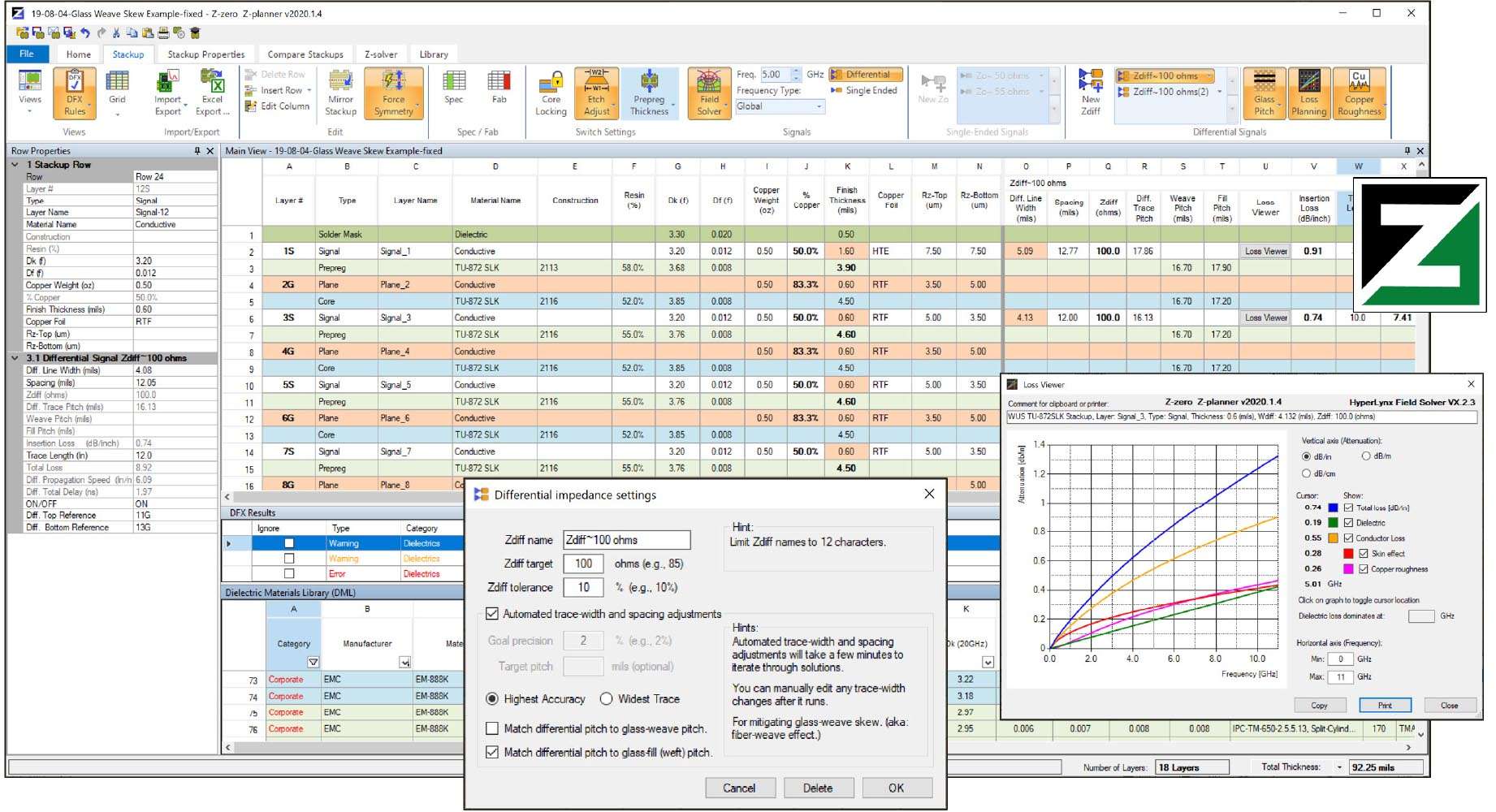
Accurate PCB stackup design is critical for ensuring signal integrity and controlling electromagnetic interference (EMI) in high-speed digital and RF circuits. Z-planner Enterprise 2025.1 provides a field-solver-based approach, moving beyond traditional rule-of-thumb methods to deliver highly precise impedance, propagation delay, and crosstalk predictions. This precision is vital for engineers tasked with designing components for applications operating at multi-gigabit speeds and high frequencies, including signal integrity, power integrity, RF/microwave, and fabrication engineers.
Electromagnetic Field Solver and Loss Modeling Capabilities
At the core of Z-planner Enterprise is an integrated 2.5D electromagnetic field solver. This solver enables detailed calculations for critical parameters such as characteristic impedance, propagation delay, insertion loss, and crosstalk. The software incorporates advanced loss modeling techniques, including conductor roughness effects using the Huray model and dielectric losses described by the Hammerstad model. By simulating these physical effects with high fidelity, Z-planner Enterprise offers superior prediction accuracy compared to conventional methods, leading to more reliable PCB designs.
Extensive Materials Library and Real-World Data Integration
Z-planner Enterprise features a comprehensive materials database populated with laminates and prepregs from leading manufacturers. This library includes frequency-dependent dielectric constant (Dk) and dissipation factor (Df) data, crucial for accurate performance modeling at high frequencies. By integrating real-world dispersion and loss characteristics, the software is well-suited for designing PCBs for demanding applications like automotive radar systems and 5G communication infrastructure where performance at elevated frequencies is paramount.
Seamless Integration with EDA and Signal Integrity Tools
To streamline the electronic design automation (EDA) workflow, Z-planner Enterprise offers robust interoperability with major design and simulation tools. It supports data exchange with leading signal integrity analysis software such as Cadence PowerSI, Keysight ADS, and SIwave, as well as PCB layout tools including Allegro, Xpedition, and Altium. This seamless integration allows for the effortless transfer of stackup definitions, improving the efficiency of both the design and simulation processes.
Manufacturing Collaboration and Fabrication-Ready Documentation
Bridging the gap between electrical design and PCB fabrication, Z-planner Enterprise generates comprehensive, fabrication-ready documentation. This includes detailed stackup drawings, precise impedance tables, and material specification sheets. The software also features an improved fabricator collaboration portal, enabling direct sharing of design data and facilitating comments and feedback. Furthermore, automated Design for Manufacturability (DFM) checks help identify potential fabrication constraints early in the design cycle, significantly reducing the risk of costly re-spins.
Latest Improvements in Version 2025.1
The 2025.1 release of Z-planner Enterprise introduces significant enhancements to support evolving industry demands. Key updates include multi-gigabit channel modeling capabilities for next-generation standards such as PCIe Gen6/7, DDR5, and 224G Ethernet. The software also features advanced copper roughness modeling enhancements for new surface treatments and an expanded materials database. Additionally, new design-for-manufacturability rules have been integrated to further optimize the fabrication process.
Frequently Asked Questions
How does Z-planner Enterprise improve PCB stackup accuracy compared to traditional methods?
Z-planner Enterprise uses an integrated 2.5D electromagnetic field solver that accurately models impedance, insertion loss, and crosstalk in multilayer PCBs. This method surpasses rule-of-thumb calculations by simulating actual physical effects, reducing errors and ensuring first-pass fabrication success.
Can Z-planner Enterprise be used for designing PCBs for 5G and automotive radar applications?
Yes, the software includes an extended materials database with ultra-low-loss dielectrics tailored for high-frequency applications like 5G and automotive radar, combined with advanced loss modeling to optimize board performance at these frequencies.
What EDA tools does Z-planner Enterprise integrate with for stackup design workflows?
Z-planner Enterprise seamlessly integrates with major signal integrity and PCB layout tools including Keysight ADS, Cadence PowerSI, SIwave, Allegro, Xpedition, and Altium, facilitating smooth transfer of stackup definitions and design data.


Reviews
There are no reviews yet.