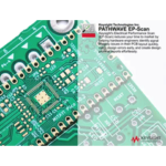
Download PathWave Electrical Performance Scan (EP–Scan) 2024 – Advance PCB Electrical Analysis Software
PathWave Electrical Performance Scan (EP–Scan) 2024, developed by Keysight Technologies, Inc., is a sophisticated Electronic Design Automation (EDA) software tool engineered for predictive and post-layout electrical analysis of Printed Circuit Boards (PCBs). It is critical for engineers working in high-speed digital design, RF/microwave engineering, and signal and power integrity analysis, enabling rigorous PCB design validation.
Overview of PathWave EP-Scan and Its Role in PCB Design Validation
Keysight Technologies’ PathWave EP-Scan 2024 serves as an essential component in the modern electronics design lifecycle. This software facilitates a “shift-left” design methodology, allowing engineers to identify and resolve electrical performance issues early in the design process, thereby minimizing costly hardware revisions. It is designed for professionals who need to ensure the electrical integrity of complex PCBs used in demanding high-speed digital and RF applications.
Advanced Electrical Performance Analysis and 3D Electromagnetic Simulation
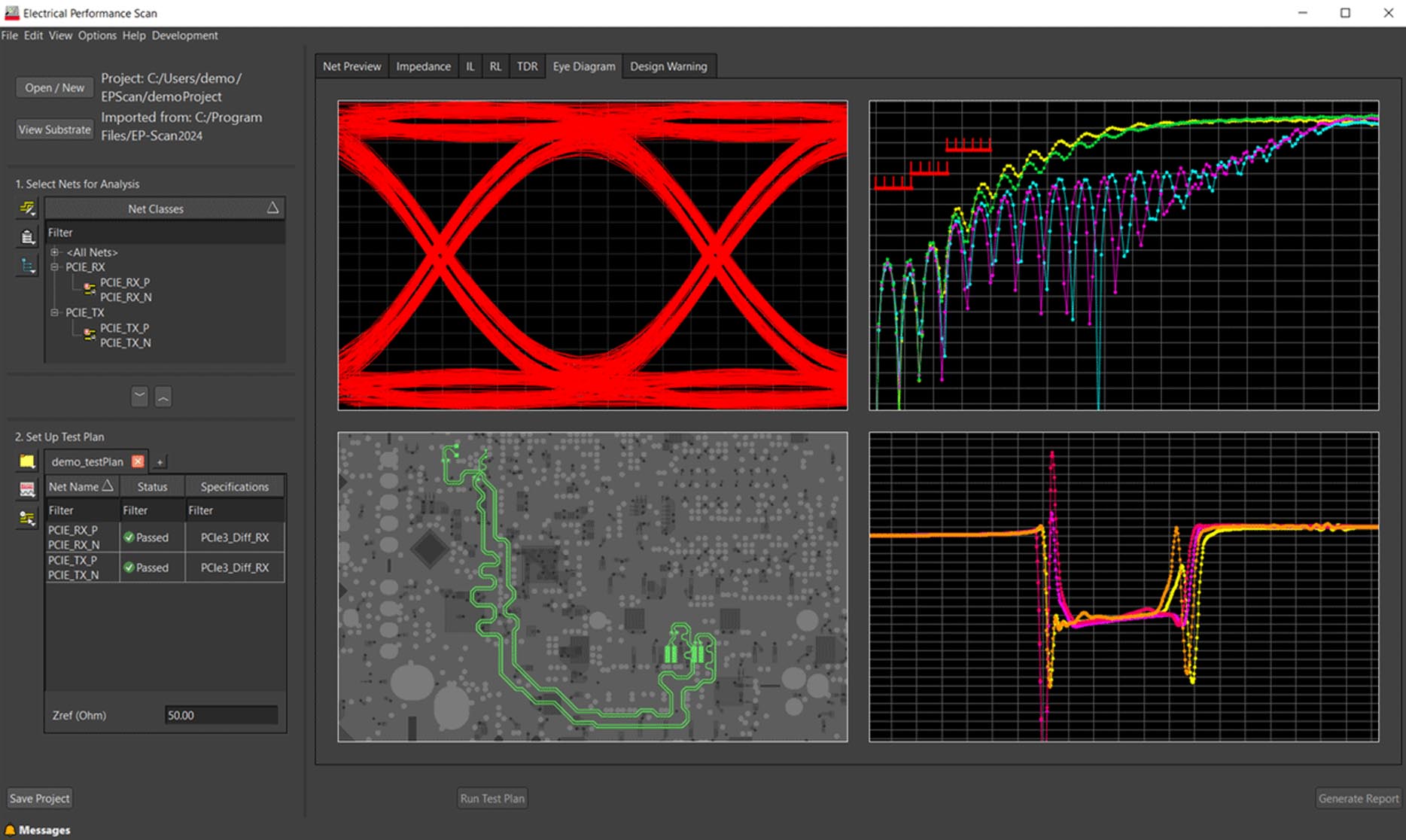
At its core, PathWave EP-Scan integrates a powerful 3D electromagnetic solver. This advanced capability enables the precise extraction of S-parameters for critical interconnects on the PCB. The tool performs in-depth analysis of signal integrity (SI) and power integrity (PI), accurately modeling phenomena such as crosstalk, impedance mismatches, insertion loss, and return loss. This allows engineers to thoroughly validate the electrical behavior of their designs before physical prototyping.
Pre-Layout and Post-Layout Verification with Industry Standard Compliance
PathWave EP-Scan supports comprehensive verification across all stages of PCB development. It can analyze designs in both pre-layout (schematic) and post-layout phases, working with standard data formats like ODB++. A key function is its ability to validate designs against stringent industry compliance standards, including those for PCIe 6.0, DDR5 memory interfaces, USB4, and various Ethernet specifications, ensuring interoperability and reliability.
AI-Powered Root Cause Analysis and Enhanced Visualization Features in the 2024 Release
The 2024 release of PathWave EP-Scan introduces significant advancements, notably its AI-driven root cause analysis. This feature leverages machine learning to intelligently diagnose and suggest probable physical causes for detected electrical rule violations, substantially accelerating the debugging process. Furthermore, the software includes enhanced visualization tools for electromagnetic fields, providing engineers with clearer insights into complex signal behavior and facilitating more efficient troubleshooting.
Cloud-Native Simulation and Workflow Integration for Scalability
To address the increasing complexity and size of modern PCB designs, PathWave EP-Scan 2024 offers cloud-native simulation capabilities. This allows users to offload computationally intensive 3D electromagnetic simulations to scalable cloud resources, significantly reducing analysis time. The software also provides seamless integration with dominant PCB EDA platforms such as Cadence Allegro, Siemens Xpedition, and Mentor PADS, streamlining workflows and enabling automated batch mode analysis for large netlists. Results are presented through a comprehensive dashboard for efficient review.
Applications Across High-Speed Digital, RF, and Signal Integrity Engineering
PathWave EP-Scan is instrumental in a variety of real-world engineering applications. Its capabilities are extensively used for SerDes channel analysis in high-speed networking, DDR memory interface validation, and PCIe channel compliance testing. RF and microwave engineers rely on it for designing and verifying complex circuit boards. Furthermore, its power delivery network (PDN) validation is crucial for advanced electronics in sectors like telecommunications, aerospace, and automotive industries, ensuring stable power distribution across high-performance systems.
Frequently Asked Questions
What types of electrical issues can PathWave EP-Scan detect on PCBs?
PathWave EP-Scan detects a range of electrical issues such as signal degradation, crosstalk, impedance mismatches, insertion and return loss, power plane resonance, and decoupling capacitor effectiveness. It enables both signal and power integrity analysis to ensure robust PCB designs.
How does the AI-driven root cause analysis improve debugging in EP-Scan 2024?
The AI-driven root cause analysis uses machine learning algorithms to suggest likely physical causes of electrical rule violations, such as problematic vias or coupling lengths, significantly speeding up the debugging process by pinpointing issues faster than traditional methods.
Can EP-Scan integrate with other PCB design tools and support cloud-based simulations?
Yes, EP-Scan integrates seamlessly with major PCB design environments like Cadence Allegro, Siemens Xpedition, and Mentor PADS. Additionally, it supports cloud-native simulation options allowing users to offload complex 3D electromagnetic simulations to scalable cloud resources for faster results.


Reviews
There are no reviews yet.