
Download Luceda Photonics IPKISS Design Suite – Advanced Photonic IC Design Automation
Luceda Photonics IPKISS Design Suite is a specialized Python-based design automation platform engineered for Photonic Integrated Circuit (PIC) development. Originating from the collaborative expertise of imec, Ghent University, and VUB, IPKISS provides engineers and researchers with a robust framework for designing, simulating, and preparing PICs for manufacturing. It caters to professionals in fields such as silicon photonics, data communications, LiDAR, sensing, and academic research, offering advanced capabilities that bridge the gap between traditional electronic EDA tools and the unique demands of photonic design.
An Overview of IPKISS and Its Role in Photonic Integrated Circuit Engineering
Photonic Integrated Circuits (PICs) are foundational for next-generation technologies, enabling light manipulation for advanced functionalities. The design of these complex circuits requires specialized tools that can handle optical phenomena and fabrication processes specific to photonics. Luceda Photonics IPKISS Design Suite was developed to meet this need, leveraging a strong academic and industrial background to create a purpose-built solution. The software supports critical applications within industries like data communications, LiDAR systems, and increasingly complex quantum photonics research.
In-Depth Photonic Design Automation Tools and Python-Based Scripting Environment
A key differentiator of the IPKISS Design Suite is its native Python programmability, which unlocks powerful automation capabilities. This environment allows engineers to:
- Develop custom scripts for intricate design tasks that are challenging in traditional GUI-based tools.
- Automate repetitive layout generation processes, including complex patterns and component arrays.
- Implement sophisticated design rule checking (DRC) tailored to specific foundry requirements.
- Conduct efficient parameter sweeps to optimize circuit performance for various operating conditions.
- Generate advanced curvilinear waveguides and other non-orthogonal geometries essential for high-performance PICs.
Integration with Foundry PDKs and Support for Industry-Standard Layout Formats
To ensure designs are manufacturable, IPKISS provides seamless integration with certified Process Design Kits (PDKs) from leading semiconductor foundries. This crucial feature allows designers to work with actual fabrication process rules and device models, increasing the predictability and success rate of tape-outs. The suite supports export to industry-standard mask layout formats, including GDSII and OASIS, ensuring compatibility with foundry manufacturing workflows. This direct integration facilitates a smoother transition from design to production, supporting the overall tape-out preparation process for PICs.
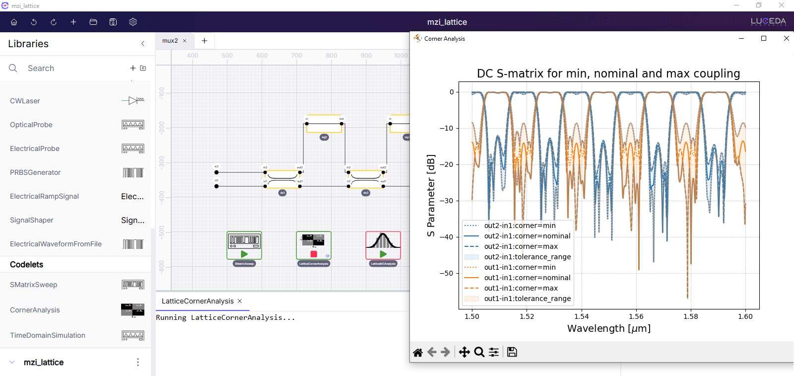
Sophisticated Circuit-Level Simulations and Co-Simulation Tools
IPKISS integrates advanced simulation capabilities essential for validating photonic circuit performance. It includes the Caphe simulator for efficient circuit-level analysis, offering rapid simulation of PICs. Furthermore, the suite provides an interactive link and bi-directional co-simulation capabilities with industry-standard photonic simulation tools such as Ansys Lumerical and Synopsys tools. This interoperability allows engineers to leverage the strengths of different simulation engines, perform detailed electromagnetic analysis alongside circuit simulations, and model advanced waveguide structures with high fidelity.
Workflow Enhancements and Collaborative Features in the 2026.03.3 Release
The IPKISS Design Suite release introduces significant enhancements designed to boost engineer productivity and design throughput. Key improvements include:
- An updated and more intuitive PDK Manager interface for easier handling of foundry process files.
- Streamlined automation features for multi-project wafer (MPW) runs, simplifying the submission process for multiple designs.
- Enhanced integration with version control systems like Git and Subversion, crucial for collaborative development and project management.
- Support for the latest Python 3.12+ ecosystem, ensuring compatibility with current development practices and libraries.
- General performance improvements across the suite, leading to faster simulation times and quicker layout generation.
Real-World Applications and Industry Use Cases
The Luceda Photonics IPKISS Design Suite is instrumental in developing cutting-edge photonic technologies. Engineers and researchers utilize it for designing components and systems in various high-impact applications. These include the development of advanced optical transceivers for high-speed data centers, sophisticated sensing systems for industrial and automotive applications like LiDAR, and complex integrated quantum photonic circuits for computing and communication. The ability to work with certified foundry PDKs also means that the suite is directly used in the industrial tape-out process, enabling commercial production of innovative PICs.
Frequently Asked Questions
What are the main advantages of using IPKISS over traditional electronic EDA tools for photonic IC design?
IPKISS is purpose-built specifically for photonics, offering native Python scripting, advanced curved waveguide support, and integration with photonic foundry PDKs, ensuring higher accuracy and repeatability tailored to photonic IC peculiarities. Traditional electronic EDA tools often lack the specialized features required for optical simulations and layout of photonic components.
How does IPKISS facilitate multi-project wafer (MPW) tape-out preparation?
IPKISS 2025.12 introduces streamlined templates for MPW shuttle runs, automates die-frame assembly, and stitch-cell placement, significantly accelerating and simplifying the complex tape-out process for multiple projects on a single wafer. This automation reduces manual effort and minimizes errors in the preparation of mask data for foundry submission.
Can IPKISS integrate with other simulation and design tools in the photonics ecosystem?
Yes, IPKISS supports direct export to Cadence Virtuoso and Synopsys OptoDesigner, and offers bi-directional co-simulation integration with Lumerical (Ansys) tools via IPKISS Canvas, enabling comprehensive simulation workflows. This allows designers to incorporate IPKISS-generated layouts and simulation data into broader design and analysis environments.


Reviews
There are no reviews yet.